


ISO Certified Multilayer PCB Assembly (Up to 32L)
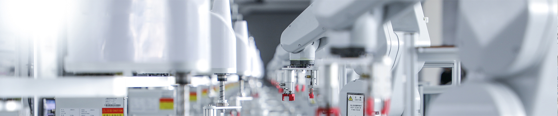
SZH has its own fully self-contained production plant with several high-precision SMT lines at the core, and additionally DIP, testing, and assembly lines. Thus, they can provide flexible manufacturing from prototype up to mass PCB assembly.
High-Precision SMT Lines: Able to mount 01005 components, 0.3mm pitch BGA, QFN, and other fine-pitch packages.
Complete Process Coverage: SMT double-sided, mixed assembly, selective soldering, and press-fit technology are all included.
Strict Quality Control: Inspection throughout the whole process with SPI, AOI, X-Ray, functional testing, and aging test systems.
- SZH
- China
- Information
Product Overview
Our multi-layer PCB assembly services offer comprehensive solutions from prototype design to mass production, specifically designed for electronic devices that require high performance, high reliability, and complex routing. With manufacturing capabilities of up to 32 layers, we are able to meet the most demanding requirements of industrial, medical, aerospace, and telecommunications applications.
Core Advantages
ISO-Certified Quality System
Certified by ISO 9001:2015 Quality Management System
Certified by ISO 14001 Environmental Management System
Full traceability throughout the entire production process
Complies with international electronic manufacturing standards
Advanced Manufacturing Capabilities
Number of Layers: 2 to 32 layers of multilayer PCBs
Board Thickness: 0.4mm to 6.0mm
Minimum Line Width/Spacing: 3/3 mils
Surface Finishes: ENIG, chemical nickel-gold, silver plating, OSP, hot air leveling, etc.
Material Options: FR-4, high-frequency materials, high Tg materials, aluminum substrates, etc.
Technical Specifications
| Parameter | Specification |
|---|---|
| Maximum Layers | 32 layers |
| Board Thickness Tolerance | ±10% |
| Minimum Hole Size | 0.15mm |
| Copper Thickness Range | 0.5oz to 6oz |
| Impedance Control | ±10% |
PCBA Assembly Capabilities
| Process | Description |
|---|---|
| Component Types | 01005, BGA, QFN, CSP, etc. |
| Placement Accuracy | ±0.025mm |
| Soldering Process | Lead-free soldering, Selective soldering |
| Inspection Technology | AOI, X-ray, Flying probe testing |
| Insulating Coating | Optional, meets IPC standards |
Application Areas
Medical Devices
Aerospace
Communication Equipment
Industrial Control
Quality Control Process
1. Incoming Material Inspection
Certified component suppliers
Traceable Material Batch System
100% inspection of key parameters
2. Process Control
Real-time SMT process monitoring
Reflow Soldering Process Curve Optimization
Electrostatic discharge protection measures
3. Final Product Testing
Functional Circuit Testing
Online Circuit Testing
Environmental reliability testing
Why Choose Us?
Expert Team
Engineers with over 10 years of experience in the PCB industry
Professional DFM analysis capabilities
7x24 hours technical support
Complete Supply Chain
Cooperation with globally renowned component suppliers
Secure inventory management system
Component replacement consultation
Confidentiality and Security
Strict confidentiality agreements
Independent customer data management
Intellectual property protection measures
FAQ
Q: What is the typical lead time for a 32-layer PCB?
A: The standard lead time is 18-25 working days, depending on design complexity and material availability.
Q: Do you support small-batch prototyping?
A: Yes, we offer comprehensive services ranging from a single prototype to mass production.
Q: How do you ensure the quality of hidden solder joints like BGA?
A: We use high-resolution X-ray inspection equipment to ensure 100% inspection of all hidden solder joints.
Q: Do you provide design support services?
A: Yes, our engineering team offers free DFM/DFA design optimization advice.


