


PCBA with AOI (Automated Optical Inspection) & X-Ray Inspection
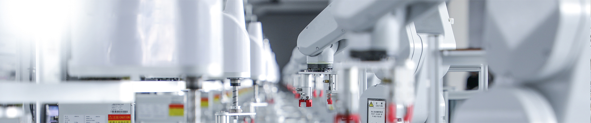
SZH has its own fully self-contained production plant with several high-precision SMT lines at the core, and additionally DIP, testing, and assembly lines. Thus, they can provide flexible manufacturing from prototype up to mass PCB assembly.
High-Precision SMT Lines: Able to mount 01005 components, 0.3mm pitch BGA, QFN, and other fine-pitch packages.
Complete Process Coverage: SMT double-sided, mixed assembly, selective soldering, and press-fit technology are all included.
Strict Quality Control: Inspection throughout the whole process with SPI, AOI, X-Ray, functional testing, and aging test systems.
- SZH
- China
- Information
Product Overview
High-Precision, High-Reliability PCBA Mainboard
Equipped with the latest advanced AOI and X-Ray inspection technologies, every mainboard is at the cutting edge of technology regarding soldering accuracy, component placement, and internal structure. Being perfect for the most demanding applications such as smart devices, industrial controls, and medical instruments, it acts as the core hardware that is a stable and reliable base for your products.
Core Technology:
1. AOI Automated Optical Inspection
Accurate Soldering Inspection: Uses high-definition cameras and intelligent algorithms to automatically detect soldering defects (such as cold solder joints, short circuits, and misalignment).
Component Placement Verification: Checks the accuracy of component position, polarity, and part number, ensuring placement precision ≥99.9%.
Real-Time Feedback and Optimization: Inspection data is synchronized in real-time with the production system, enabling closed-loop process control.
2. X-Ray Non-Destructive Testing
Internal Structure Visualization: Provides 3D imaging of hidden solder joints (such as BGA and QFN), eliminating concealed defects.
Multilayer PCB Analysis: Accurately inspects internal circuit connectivity, via wall integrity, and layer alignment.
Material Integrity Verification: Detects tiny defects such as internal component cracks or voids.
Technical Specifications
| Parameter | Specification |
|---|---|
| Board Material | FR-4 / High-Frequency / Aluminum Base (Customizable) |
| Maximum Layers | 1-20 Layers |
| Min. Line Width/Space | 0.05mm / 0.05mm |
| Surface Finish | ENIG, HASL, OSP, Immersion Silver |
| Soldering Technology | Lead-free, RoHS compliant |
| Test Coverage | 100% AOI Full Inspection + Targeted X-Ray Inspection |
Application Fields
Industrial Control: Industrial computers , sensor modules.
Medical Devices: Patient monitors, diagnostic equipment, portable medical devices.
Consumer Electronics: Smart home, IoT terminals, high-end audio.
Automotive Electronics: Vehicle control systems, electric vehicle battery management systems.
Communication Equipment: 5G modules, routers, base station units.
Main Advantages
Zero Defect Orientation: Dual inspection technology reduces potential failure rates to ≤0.01%.
Long-Term Reliability: Precision engineering ensures stable performance under extreme temperature and humidity conditions.
Fast Delivery: Automated testing improves production efficiency, supporting flexible small to medium batch customization.
Comprehensive Traceability: Each circuit board comes with an inspection report, with data traceable to the production batch.
Precision Inspection, Reliable Assurance
Choosing us means choosing a steadfast commitment to quality, ensuring that every PCBA board becomes a solid foundation for the success of your product.


