


Custom Embedded System PCBA Design and Low-Volume Manufacturing
SZH has its own fully self-contained production plant with several high-precision SMT lines at the core, and additionally DIP, testing, and assembly lines. Thus, they can provide flexible manufacturing from prototype up to mass PCB assembly.
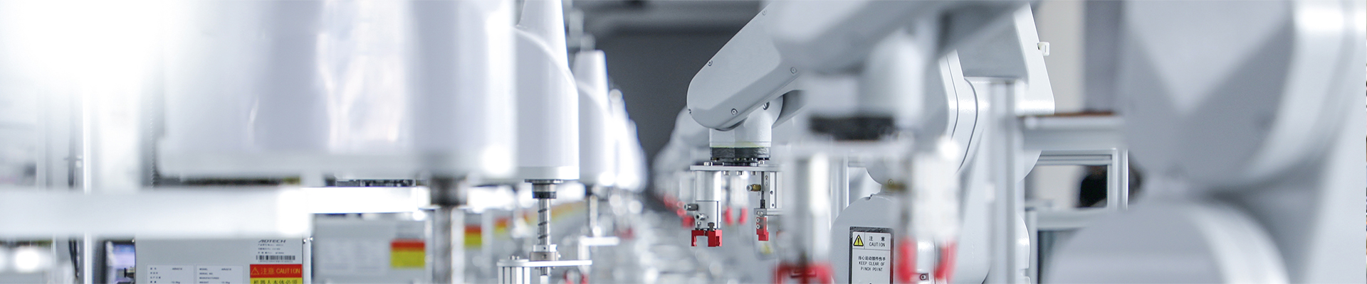
High-Precision SMT Lines: Able to mount 01005 components, 0.3mm pitch BGA, QFN, and other fine-pitch packages.
Complete Process Coverage: SMT double-sided, mixed assembly, selective soldering, and press-fit technology are all included.
Strict Quality Control: Inspection throughout the whole process with SPI, AOI, X-Ray, functional testing, and aging test systems.
- SZH
- China
- Information
Custom Embedded System PCBA Design and Low-to-Large Volume Manufacturing
1. Core Value
End-to-End PCBA Solution Engineered for Innovative Hardware
We turn your ideas into dependable, working hardware. From initial architecture through to the finished board, our turnkey service for custom embedded system design and low-volume manufacturing not only helps but makes your prototype - production transition go smoothly.
2. Technical Capabilities
Excellence in Low-Volume Production
Flexible Low-Volume Production: Economical production batches ranging from 10 to 10,000 units..
Multi-Material Expertise: FR-4, high-frequency Rogers, flexible PCBs, and more.
Advanced Assembly: fine-pitch BGAs (0.35mm), QFN, PoP, and other complex packages.
Complex Multilayer PCBs: Capable of producing HDI (High-Density Interconnect) boards with up to 24 layers.
Strict Quality Control: Full range of inspections, including AOI, X-ray inspection, and ICT.
3. Application Solutions
Industry-Specific Applications
Industrial IoT: Edge computing gateways, sensor hubs, device monitoring modules.
Medical Devices: Portable diagnostic devices, patient monitoring systems, medical imaging preprocessors.
Consumer Electronics: Smart home controllers, core boards for wearable devices, dedicated interactive devices.
Automotive Electronics: Telematics control units, advanced driver assistance system modules, in-vehicle infotainment systems.
Communications: Dedicated protocol converters, network edge nodes, specialized wireless modules.
4. Quality Assurance
Three-Level Quality Control
Design Verification: DFM/DFA, SI/PI analysis and so on.
Process Control: Incoming, in-process, and final inspection.
Product Validation: Functional, performance, environmental, and aging testing.
5. Why Partner With Us
Key Differentiators
In-depth Collaboration: Direct communication between engineers.
Transparent Process: Real-time project tracking with key stages signed off by the client.
Cost-Optimized Design: Balancing performance and manufacturing economy from the start.
Evolvable Design: Hardware version strategy to simplify future upgrades.
7. Technical Specifications Overview
| Capability | Range |
|---|---|
| PCB Layers | 1-24 layers (HDI capable) |
| Min. Trace/Space | 3/3 mil |
| Operating Environment | Temperature: -20°C to 85°C, Humidity: 10%~90% non-condensing |
| Min. Hole Size | 0.15mm (mechanical), 0.1mm |
| Testing | Flying Probe, ICT, Functional Test, Boundary Scan |
Contact Our Engineering Team
Participation in the facilitation of your hardware innovation from vision to realization is what we are ready for!


